High Speed FPGA PCB
In progress · Planning
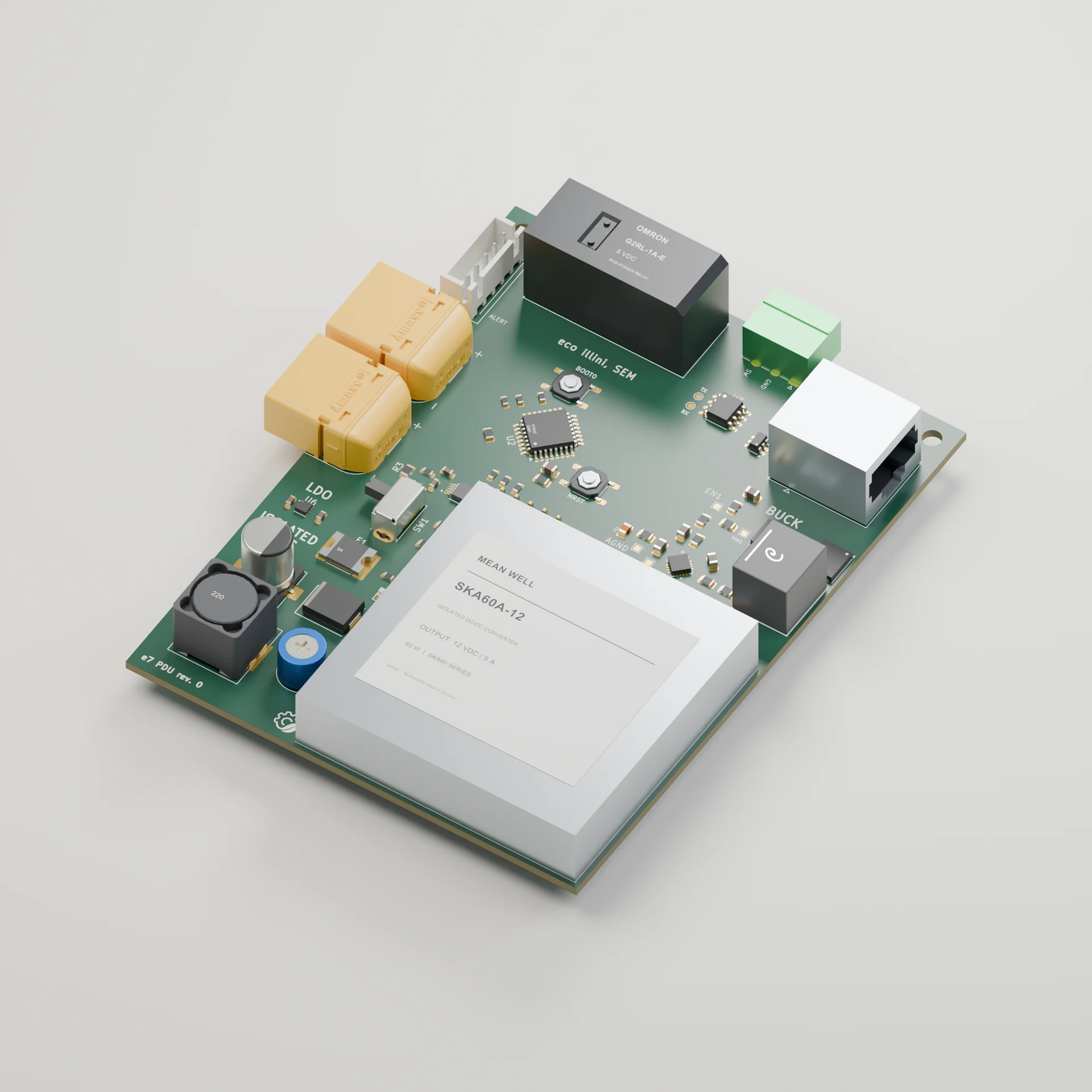
Planning a custom FPGA board with external DDR memory, several power rails and debug access, to learn how those constraints shape a board before fabrication.
Open questions
- Which FPGA and memory pairing can be routed and assembled?
- How should four low-voltage rails start up from 5 V?
- What test access will isolate a first-power fault?